PCB Thermal Copper Area February 16, 2007
I published the following Zoho Sheet to calculate the PCB copper surface area to cool a device based on its power dissipation.
It is embedded below and can also be opened in its own window.
Tips to Avoid Arcing December 19, 2006
I have gotten several requests for information about high voltage PCB design and how to avoid arcing.
For example, Ken writes:
“Could anyone explain surface arcing causing hi-pot test failure?”
I thought I would make a short post to serve as a place to discus these issues.
(more…)
Current vs. Trace Thickness and Temperature vs. Copper Density December 15, 2006
Regarding the PCB Trace Width Calculator [1], Regit asks:
(a.) What is the relationship between current and trace thickness? And, (b.) what is the relationship between temperature and copper density?
Answers: (more…)
Reducing EMI in PCBs December 6, 2006
I got the following question by email:
When a data sheet says “minimize the trace area for lowest EMI”, do they mean thin trace? Does higher reactance minimize EMI?
It is a good question, so I though I would post something on this.
Minimizing EMI requires minimizing the electric and magnetic fields around the trace. If a trace has a lot of voltage that is changing fast, it will tend to emit a strong electric field. In such a case, making the trace have less surface area can help limit the emissions. Better yet, shielding the noisy trace with a trace that lets the energy return to where it came from is very effective - the shorter the return path, the better. In fact, if the noisy trace is completely surrounded by the shield, the electric field lines won’t get out and the noise will be contained. Once shielded, the area of the trace is not so critical in terms of noise, however more area also means more capacitance, which your circuit may not like. Therefore, yes, it is usually a good idea to minimize the area of an E-field emitting trace, but it must be able to carry the needed current of course.
Next is the magnetic field, which comes from a changing current. The higher the current and the faster it changes, the worse the EMI can be. The magnetic field can be somewhat canceled by routing the returning current as close as possible to the outgoing current. In other words, the loop area traveled by the current needs to be small. We are talking about AC current here, so it can be contained to a small area by effective use of decoupling capacitors. These should be placed near the source of the noise current.
Ground planes can help contain both electric and magnetic fields. They give the electric field lines a place to terminate, and those high frequency return currents will automatically flow near the outgoing currents due to an imaging effect where the ground plane will actually mirror the trace currents with currents flowing in the opposite direction.
Shortcomings of the IPC-2221 Current Capacity Guidelines October 31, 2006
Our friends at Flomerics have posted an interesting article [1] that describes some of the shortcomings of the IPC-2221 design rule for determining the current carrying capacity of PCB traces. The article concludes that the IPC rule is based only on a 1.6 mm thick, 2-sided FR4 board with a single trace on one side, solid copper on the back side, and 35 um of copper sheet thickness. Modern PCBs can typically have a lot more layers and more copper, and thus be able to take more current with less temperature rise in the traces due to better heat spreading and better heat shedding. The author then derives a new series of graphs showing the temperature rise vs. current and trace width for various PCB stack-ups. Also, it seems that internal layers can handle a lot more current than IPC-2221 would have us think.
[1] New Correlations Between Electrical Current and Temperature Rise in PCB Traces, Johannes Adam
http://www.flomerics.com/flotherm/technical_papers/t341.pdf
Conductive Ink Traces June 14, 2006
Conductive ink, for example the Dow Corning PI-2000 series of Silver Polymeric Interconnect Materials, can be used to print conductive circuit traces. Generally, the ink is applied using a screen printing technique, with typical print thicknesses of 25 um to 40 um. Sheet Resistivity is specified in milliohms/square at a 25 um print thickness and varies from 8 to 81 for the currently available inks. For comparison, copper has a Sheet Resistivity of 0.68 milliohms/square at a 25 um thickness.
The Sheet Resistivity can be used to calculate the resistance of the printed traces as follows:
Resistance = Sheet_Resistivity*(Length/Width)*(Ref_Thickness/Thickness)
where "Ref_Thickness" is the thickness at which the "Sheet_Resistivity" is specified in the ink's data sheet and "Thickness" is the actual thickness of the ink you are printing.
The Calculator
(more...)
PCB Via Thermal Resistance May 22, 2006
By popular demand, I’ve also added thermal resistance calculation to the PCB Via Calculator. Thanks for the good suggestions!
PCB Trace Thermal Resistance May 17, 2006
I had a request to calculate the thermal resistance of a PCB trace, so I updated the trace resistance calculator to add this feature.
Find PCB Trace Width Based on Power April 20, 2006
I had a request for a calculator to find the width of a PCB trace based on its voltage drop or power dissipation. This time I am trying something new. I made the calculator as an Excel Spreadsheet and posted it on Zoho Sheet. Let me know how the Zoho Sheet works for you.
Note that there are two tabs - one for voltage drop and one for power dissipation. The sheet is embedded below or can be opened in its own window by clicking the following link:
https://www.zohosheet.com/public.do?fid=3083Making AutoComplete Work with Cut and Paste April 12, 2006
In Internet Explorer, the AutoComplete feature for forms can be handy, but I have noticed that it doesn’t work if you cut and paste text into the form. On the other hand, if you manually type text into the form, it is remembered. I found that you can force AutoComplete to work with cut and paste by deleting the last character and retyping it. This is a great time saver – especially for things like tracking numbers.
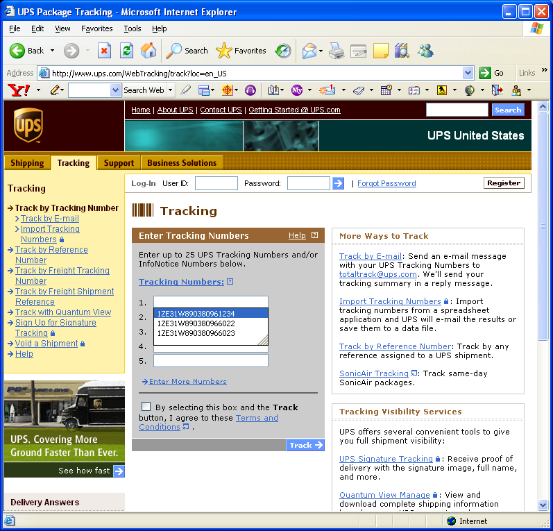
Also note that you can delete a single item from the AutoComplete drop down by selecting it and pressing delete.
« newer posts | older posts »