3-Phase Calculations January 5, 2008
Here is a Zoho Sheet to do various 3-Phase calculations. It can convert between line-to-line and line-to-neutral voltages, find current based on apparent power (KVA), and choose the required wire cross sectional area to meet the target voltage drop. When designing such a system, you must also meet all applicable laws and safety codes.
It is embedded below (more…)
Wire Parameter Calculator September 20, 2007
This Javascript web calculator will calculate the resistance and ampacity for copper wire based on the gauge. Both metric (mm) and American Wire Gauge (AWG) are supported. Note: Ampacity is based on a curve fit to MIL-STD-975. To see the wire table that this calculator is based on as well as important information about wire insulation temperature ratings, click here.
Features:
- Results update as you type
- Several choices of units
- Units and other settings are saved between sessions
- Blog format allows user comments
Inputs:
| Wire Size |
Optional Inputs:
| Wire Temperature | Deg. | |
| Wire Length | ||
| Number of Wires in Bundle |
Results (per each wire):
| Resistance | Ohms | |
| Single Wire Ampacity | Amps | |
| Wire Bundle Ampacity (per wire) | Amps | |
| Copper Diameter | ||
| Copper Area | ||
| Copper Weight |
Hex, Decimal, and Binary Converter June 29, 2007
This web calculator converts numbers between the hexadecimal (hex), decimal, and binary formats. The calculator was designed to allow easy conversion between any of these three formats. This task is very common for those working with digital hardware and software including microcontrollers, DSP’s, FPGA, etc. (more...)
Skin Effect Calculator June 18, 2007
Electrical current always flows in the path that results in the lowest expenditure of energy. At lower frequencies, current flows in a path that reduces I^2*R losses. This is the path of shortest distance and is fairly intuitive to think about.
At higher frequencies, things get a little strange. (more...)
PCB Stack-Up Design And Impedance Calculator May 12, 2007
Review: A new PCB stack-up design and impedance calculator is available for download from Istvan Nagy (see link below). It is a full-featured Excel-based tool that helps plan the PCB stack-up so that controlled impedance traces can be effectively implemented. It covers both single-ended and differential traces and is based on the equation s from IPC-D-317A. It allows one to see the range of impedances that are possible for a given layer stack-up. It also has pre-distortion calculations to support high-speed compensation, a unit changer, and a materials library.
Right-Click, Download and Save the Excel tool here:
layerstack_planningoriginalipc.xls
Istvan Nagy’s home page:
[Sorry, link had to be removed due to content issues.]
Do you have a favorite stack-up and impedance calculation tool? Let us know about it in the comments below.
Transmission Line Calculator March 6, 2007
The Excel based tool (see link below) calculates the capacitance and inductance per unit length as well as the impedance of a transmission line. It may be applied to wires, PCBs, etc. (more…)
PCB Thermal Copper Area February 16, 2007
I published the following Zoho Sheet to calculate the PCB copper surface area to cool a device based on its power dissipation.
It is embedded below and can also be opened in its own window.
Conductive Ink Traces June 14, 2006
Conductive ink, for example the Dow Corning PI-2000 series of Silver Polymeric Interconnect Materials, can be used to print conductive circuit traces. Generally, the ink is applied using a screen printing technique, with typical print thicknesses of 25 um to 40 um. Sheet Resistivity is specified in milliohms/square at a 25 um print thickness and varies from 8 to 81 for the currently available inks. For comparison, copper has a Sheet Resistivity of 0.68 milliohms/square at a 25 um thickness.
The Sheet Resistivity can be used to calculate the resistance of the printed traces as follows:
Resistance = Sheet_Resistivity*(Length/Width)*(Ref_Thickness/Thickness)
where "Ref_Thickness" is the thickness at which the "Sheet_Resistivity" is specified in the ink's data sheet and "Thickness" is the actual thickness of the ink you are printing.
The Calculator
(more...)
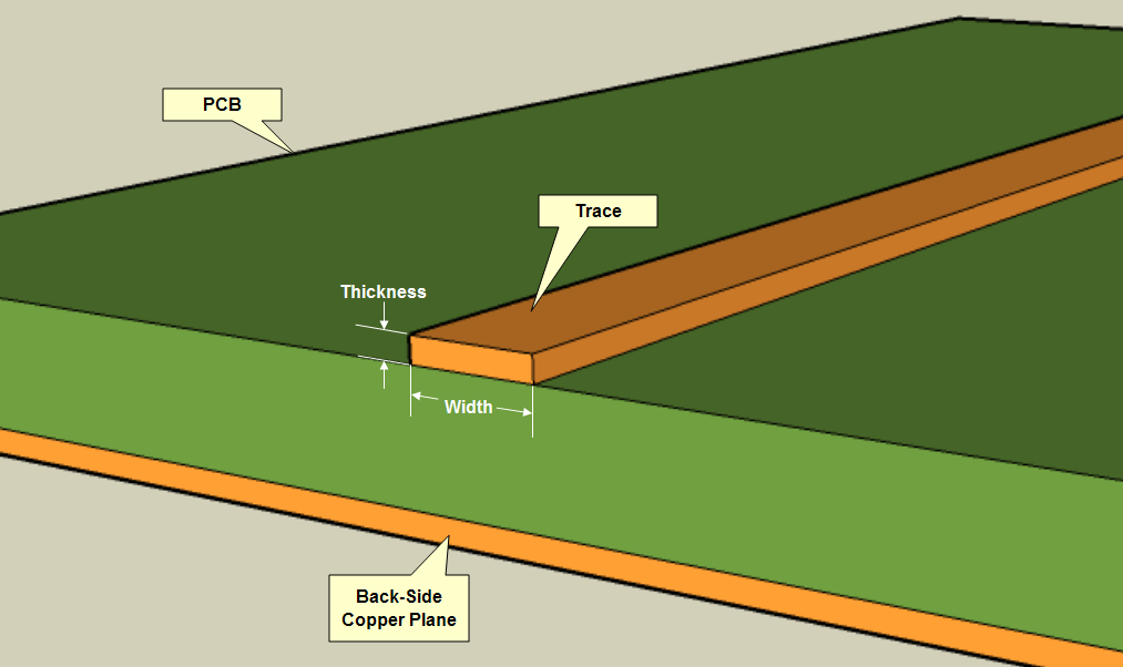
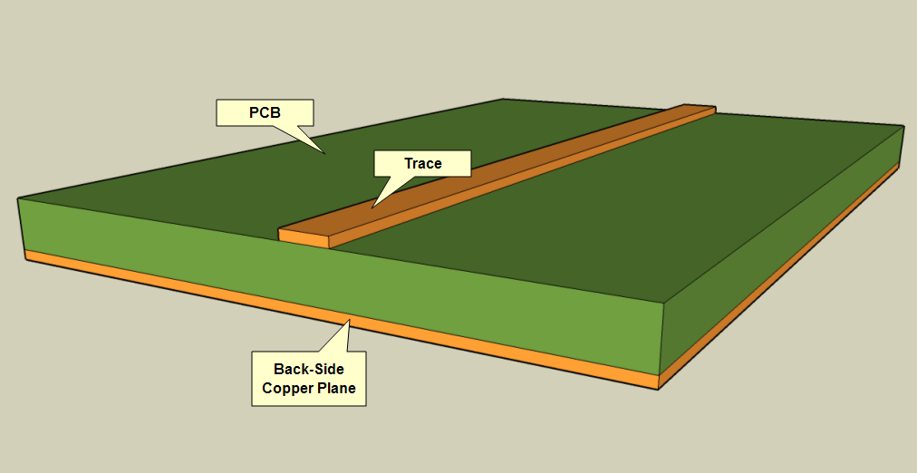
PCB Trace Width Calculator January 31, 2006
This Javascript web calculator calculates the trace width for printed circuit boards based on a curve fit to IPC-2221 (formerly IPC-D-275). Also see the via calculator.
New features:
- Results update as you type
- Several choices of units
- Units and other settings are saved between sessions
- Blog format allows user comments
Inputs:
| Current | Amps | |
| Thickness |
Optional Inputs:
| Temperature Rise | Deg | |
| Ambient Temperature | Deg | |
| Trace Length |
Results for Internal Layers:
| Required Trace Width | ||
| Resistance | Ohms | |
| Voltage Drop | Volts | |
| Power Loss | Watts |
Results for External Layers in Air:
| Required Trace Width | ||
| Resistance | Ohms | |
| Voltage Drop | Volts | |
| Power Loss | Watts |
Notes:
The trace width is calculated as follows:
First, the Area is calculated:
Area[mils^2] = (Current[Amps]/(k*(Temp_Rise[deg. C])^b))^(1/c)
Then, the Width is calculated:
Width[mils] = Area[mils^2]/(Thickness[oz]*1.378[mils/oz])
For IPC-2221 internal layers: k = 0.024, b = 0.44, c = 0.725
For IPC-2221 external layers: k = 0.048, b = 0.44, c = 0.725
where k, b, and c are constants resulting from curve fitting to the IPC-2221 curves
For geometry diagrams, click on the pictures below.
For frequently asked questions, see the comments.
PCB Trace Resistance Calculator January 24, 2006
This online web calculator finds the resistance of copper PCB traces (a.k.a. tracks) of given width, thickness, length, and temperature. It can also be used for copper bars (e.g. bus bars). Several choices of common units are available. Enter the Width and Thickness below. Optionally, enter the Temperature and Length, or just leave the default values. (To find the needed trace width based on current, see the PCB Trace Width Calculator.)
May 17, 2006 - Added (lateral) thermal resistance calculations.
January 18, 2007 - Clarified equations.
The Calculator
(more...)